INTRODUCTION
Since the first
point-contact bipolar transistor, invented in 1947, there has been much
progress in the development of very high density integrated circuits (IC),
often referred to as very large scale integration (VLSI).Although many new
devices have been invented, the bipolar transistor is still one of the key
devices in every IC. Bipolar devices offer the following advantages compared to
CMOS: high current drive ability, high frequency response, good matching,
analog applications, low noise and high trans-conductance. Diffusion and ion implantation are the
two key processes to introduce a controlled amount of dopants into
semiconductors and to alter the conductivity type. In the fabrication of
semiconductor devices, the diffusion process must give repeatable, controlled
value of impurity concentration and depth of diffusion. This requires accurate
control temperature, the impurity surrounding the slice and duration of the
process. Typically the diffusion process can be divided into two stages called
pre-deposition or deposition and drive-in.
Manufacture
of Junction Transistors
As most
of the transistors used at present in radio receivers are made by the
alloy-junction method, only this technique will be described. For the same
reason, it will not be necessary to consider the production of n-p-n, silicon,
or high-power transistors. The descriptions which follow therefore apply to
germanium p-n-p transistors in general, and in particular to small-signal r.f.
and a.f. transistors and medium-power output transistors.
Thus the present article will be concerned primarily with the OC44
and OC45 r.f. transistors; the OC70 and OC71 a.f. transistors; and the OC72,
OC78 and OC81 a.f. output transistors. To cover the production of a range of
transistors it is necessary, of course, to concentrate on those processes which
are common to all the types.
The a.f. transistors just listed - the OC70, OC71,
OC72, OC78 and OC81 - have a similar basic construction, the cross-section of
which is represented diagrammatically in Fig. 1. The base layer is square or
rectangular. The construction of the OC44 and OC45 differs from this in that
the base wafer is round and the connection to the base layer is made by a
ring-shaped tab which surrounds but does not make contact with the emitter
pellet.
These basic constructions, although at first sight comparatively
simple, involve many complex techniques, many of which in the past have been
confined to the research laboratory. These intricate laboratory processes are
now applied to quantity production in the Mullard transistor factories.
RAW MATERIAL
The
most important raw material used in transistor manufacture is germanium. There
are several interesting sources of this rare metal.
Germanium is present in small proportions in the copper-bearing
ores of the Katanga region of the Congo. It also occurs associated with zinc in
S.W. Africa. Another source, and not the least romantic, is the flue dust
produced by burning Northumbrian coal.
Northumbrian coal contains about 0.02% of germanium. This is
equivalent to about 1 ounce in 3 cwt. Burning the coal acts as the first stage
in the extraction, the resulting flue dust sometimes being as much as 1 to 2%
rich in germanium.
The subsequent extraction of the germanium follows normal
industrial-chemical practice. The germanium comes to the transistor factory in
the form of germanium dioxide-a white powder. By heating the germanium dioxide
for several hours in an atmosphere of hydrogen gas, the powder is reduced to
the metal germanium.
HIGH DEGREE OF PURITY
Chemical
analysis would show the resulting germanium to be quite pure. But for
transistor manufacture, a degree of purity higher than for any other
manufactured article is required.
Traces of impurity have an all-important effect on the conductive
properties of germanium. The nature of the impurities and their concentration
in the germanium have to be rigorously controlled. Otherwise the electrical
properties will be unpredictable, and the germanium will be unsuitable for
transistor manufacture.
The purification is completed by a process known as zone refining.
The refining is continued by this process until the impurities with electrical
activity are reduced to the order of one part in ten thousand million-1 in
10^10. Put the other way, the germanium is 99.999 999 99% pure.
This degree of purity was unheard of in metal working before the
development of semiconductor devices. The impurity level, which is right
outside the range of chemical analysis, is tested by checking the resistivity
of the material.
ZONE REFINING
The
ultimate degree of purity is achieved by zone refining. This process is based
on the fact that impurities will concentrate more readily in the molten rather
than in the solid metal. The zone refiner consists of a silica tube surrounded
at intervals by r.f. heating coils. The bar of germanium, after being etched in
chemicals to remove the scale from the outside, is placed in a graphite boat
and inserted into the zone refiner.
The graphite boat containing the ingot of germanium is drawn
slowly through the tube. Each r.f. heating coil heats up the graphite boat by
induction, and thus creates a zone of molten germanium. As the ingot passes
through the coils, the zones travel the length of the bar. The impurities
collect in the molten zones and are swept to one end of the bar.
The principle of the process is illustrated in Fig. 2, which for
the sake of simplicity is drawn for only one molten zone.
Fig.2
RESISTIVITY CHECK
The
purity of the germanium is checked by measuring its resistivity. A small flat
is ground along the length of the bar.
Along this flat the resistivity of the bar is measured, centimetre
by centimetre. The measurement is made by means of a probe having four prongs.
The two outer prongs apply a known current, and the voltage drop is measured
across the two inner ones.
The greater the amount of impurity, the lower the resistance. At
the end of the ingot containing the impurities from the zone refining, the
resistance drops considerably. The point at which the resistance becomes too
low is marked on the bar, and this end is cut off by a diamond-impregnated
wheel and discarded.
LEVELLING
The
initial purification is designed to eliminate unwanted imperfections from the
lattice. Subsequent doping ensures that the imperfections are only such as to
give the required p- or n-type conduction.
The germanium in the ingot will eventually be formed into the base
wafers of p-n-p transistors. Consequently this germanium needs to be made
n-type, so that it will have free negative carriers.
A known concentration of antimony must therefore be added to the
germanium in the bar. The concentration of the antimony is to be about 1 part
in 10^8. The process of introducing the antimony is known as levelling. This
process is modified in such a way that the germanium is at the same time
re-crystallised as a single crystal.
The ingot of germanium as it comes from the zone refiner consists
of many small crystals of different sizes, the axes of which are arranged at
random. It is poly crystalline. Any sample taken from the ingot will consist of
pieces from various crystals. Unwanted imperfections would therefore be present
in the sample at the boundaries between the crystals.
For consistent electrical properties, the ingot has to be
transformed into a single crystal. To perform the combined operations of
levelling and recrystallisation, the rod of pure germanium is placed in a
silica boat lined with graphite. A short length of single-crystal germanium,
produced during a previous refining, and known as the seed, is placed at one
end of the rod. Between the seed crystal and the rod, small weighed pellets of
antimony are inserted.
The levelling and recrystallisation now proceeds by a process
similar to zone refining, but using only one molten zone. The metal in the boat
is heated by the currents induced in a ring of graphite. As the boat is drawn
through the heated zone, a single crystal of germanium grows from the seed. By
choosing the right width and speed for the zone, the antimony becomes evenly
distributed throughout the length of the bar.
A single crystal of n-type germanium is produced in this way. It
is extremely hard, almost as hard as glass, and is usually cut with a diamond.
It cannot be scratched with a steel blade. Before the next operation, the
mono-crystalline bars are measured for resistivity, again using the
four-pronged probe.
SLICING
The
n-type monocrystalline germanium is required in the form of small, thin wafers.
At a later stage in the manufacture, the p-type additive (indium) is infused
into two regions on opposite faces of the wafer, to form the emitter and
collector. The remaining non-infused germanium in the wafer will constitute the
base region.
The base of the transistor has to be extremely thin, and although
the effective thickness is governed finally by the depth of infusion of the
indium additive (Fig. 1), it is necessary to obtain thin slices in the first place.
The rod of n-type germanium is cut into short lengths which are
mounted on a plate and waxed to hold them firmly in position. These portions
are now cut into sections or slices about half a millimetre thick. The cutter
works rather like a miniature bacon sheer, but is equipped with several
diamond-impregnated cutting wheels. The crystal is set at the correct angle in
the cutter by means of x-rays. The cutting operation is automatic.

Removing slices of crystal after grinding.
LAPPING
The
slices obtained from the cutting machine are separated from each other and the
wax is dissolved. The faces of the slices are now ground to remove those parts
of the crystal which have been fractured by the diamond cutters. This is the
lapping process. Lapping produces an incidental reduction in the thickness of
the slices.
The slices are separated by spacers in the lapping machines and
are ground by successively finer abrasives. After lapping, the resistivity of
the slices is measured, and they are sorted into groups suitable for various
transistor types.
Measuring the resistivity of germanium slice.
DICING
|
Slices of germanium are seen here being cut into small
circular wafers by an ultrasonic drill. The wafers,
after they have been etched to reduce their thickness
still further, will form the base region of transistors.
|
The
cross-sectional area of the slices is quite large. Each slice, in fact, is cut
up to form a large number of base wafers.
The base wafers are square, rectangular or round, according to the
type of transistor being made.
Square or rectangular wafers are required for the small-signal and
medium - power a.f. transistors. For the OC81, the wafers have to be 2.4 x 2.4
mm, that is, about a tenth of an inch square.
The cutting of the slices is known as dicing. The slice passes
under diamond cutters which score a parallel set of grooves on it. The slice is
turned automatically through 90° at the end of the run. On the return journey,
more score marks are made at right angles to the first marks. The resulting
criss-cross of grooves, rather like those on a bar of chocolate, allows the
slice to be separated easily into single wafers.
Round base wafers, 1.45 mm in diameter, are required for the OC44
and OC45 production. These wafers are obtained from the slices by means of an
ultrasonic drill fitted with a perforated bit.
ETCHING
The
final reduction in the thickness of the base wafers is made by etching. The
wafers are placed in a small polythene basket with numerous small holes in its
side and bottom, and the basket is agitated in the etching fluid.
After this first etch, the wafers are automatically coarse-graded
into batches according to their thickness. Each batch is then re-etched for a
period of time depending on the average thickness of the wafers in the
batch.
After the second etch, the wafers are fine graded. Further
corrections to the thickness are not carried out by etching, instead, in the
subsequent alloying, the temperatures of the furnace are adjusted to suit the
average thickness of the wafers in each of the fine grades.
The thinnest base wafers are those produced for the OC44 and
OC45.These wafers are only 100 µm thick - a tenth of a millimetre. At this
still quite early stage in manufacture, the dice are worth more than their
weight in gold.
PELLETS
To
form the p-type emitter and collector regions, pellets of a p-type additive
have to be fused to each side of the n-type base wafer. The p-type additive
chosen is indium.
Indium is a silvery metal, classed as a rare metal like germanium,
and sufficiently soft to mark paper as do lead and graphite. Indium wire or
strip is cut into portions containing the amount of material required for the
pellets. The pellet which forms the Collector is three to five times the size
of the one used for the emitter, according to the type of transistor.
The process for shaping or 'balling up' the pellets bears some
resemblance to that used for making lead shot. The pieces of indium are dropped
down a glass tube about three feet high and filled with liquid. At the top the
liquid is sufficiently hot to melt the pieces of indium into droplets. Further
down the liquid is cooler and the drops of indium solidify into spherical
pellets.
ALLOYING
The
alloying of the collector junction is carried out before that of the emitter
junction. The collector pellet, the base wafer, and the base tab, previously
tinned, are assembled in a jig. A moving belt carries the jigs through an
electric furnace, the temperature of which is higher than the melting point of
indium but lower than that of germanium. The molten indium penetrates the
germanium to form an alloy of p-type germanium which is in intimate contact
with the n-type base material.
The jigs are now removed from the furnace, loaded with emitter
pellets, and passed once more through the furnace.
The furnace is divided into three temperature-controlled zones, the
temperatures being controlled to within ±1°C on temperatures of the order of
650 °C. This close control is necessary because the depth of alloying, and
hence the effective thickness of the base, depends on the furnace temperature.
SOLDERING
Although
the germanium wafers with their alloyed pellets can now be considered to be
true transistors, many operations remain to be performed before they can be of
any practical use.
The first of these operations consists in connecting the
semiconductor material to leads passing through a glass foot by means of jumper
wires. The tinned jumper wires have to be soldered to the emitter, base and
collector regions of each unit-an extremely critical operation. Even a
miniature soldering iron would be difficult to handle on such small components,
and might introduce unwanted impurities. Instead, a stream of hot gas often
serves as a source of heat. For the assembly of other types, the heat is
provided by discharging a capacitor through the jumper wire. To ensure that the
jumper wires are attached accurately to the emitter and collector pellets, the
soldering is carried out under a microscope.

The job of joining wires to the emitter and collector pellets is so delicate
that
binocular microscopes are used. After joining, the devices are hung from a
magnetic conveyor belt in a washing trough for dispatch to the following
process.
CLEANSING AND ETCHING
After
the intricate soldering operation, the flux is washed off by de-ionised (and/or
demineralised) water, and the assembly is etched. The etching removes surface
contamination, and prevents short circuits from occurring across the emitter and
collector junctions at the points where the non-alloyed residue in the indium
pellets meets the base material.
The assembly is submitted to a further wash in demineralised water
to remove the chemicals used for etching, and then passes through a drying
oven.
ELECTRICAL PRE-TEST
Before
the transistors are encapsulated, they undergo an electrical pretest. To
prevent contamination, the pre-test is made in a hermetically-sealed dry box
containing a nitrogen atmosphere of controlled humidity.
ENCAPSULATION
The
transistors are now ready for placing in their glass bulbs. The envelopes are
first filled with a special silicone compound which will protect the transistor
from moisture and help to conduct heat away from the semiconductor material.
The seal between the glass bulb and the foot is made either by
electrically generated radiant heat, or by a gas flame on equipment looking
like a scaled-down valve-making machine.
LEAK TEST
Sample
transistors are double tested for ineffective seals. In the first leak test,
the transistors are submerged in a mixture of methylated spirit and red dye.
The penetration of the red dye into the envelope reveals transistors suffering
from gross leakage.
The second leakage test is really a tropical test, to which again
sample transistors are submitted. The test lasts three days, during which the
transistors are subjected to three on/off cycles of high temperature and high
humidity. If the envelope is at all leaky, the performance of the transistor
will deteriorate markedly and it will be rejected at the final electrical test.
It only remains for the bulb to be painted, or fixed in a metal
can, and for the type number and other marks to be applied. Although the
spacing of the leads indicates which is for the emitter, base or collector, a
coloured spot is placed on the case opposite the collector lead for greater
ease of identification.
QUALITY CONTROL
A
comprehensive system of quality control is applied throughout the manufacturing
process. On completion, the transistors undergo a series of exhaustive tests.
In this way, Mullard engineers ensure that only transistors of the highest
quality and reliability reach the consumer.
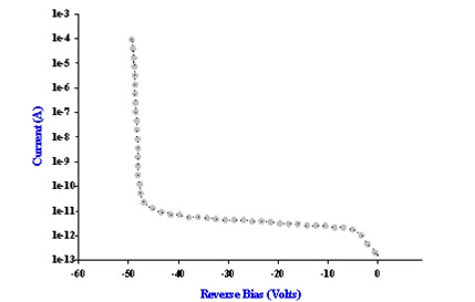
RESULTS AND DISCUSSION
Among
semiconductor devices, the bipolar junction transistor is the most sensitive to
material quality andprocessing defects. Therefore, the bipolar transistor,
along with p-n junction diode, was fabricated on SOI substrate in order to use
different dopant of solid-state source diffusion such as Boronplus and
Phosphorusplus concentrations using deposition and derive-in process at room
temperature. After fabrication, device was tested using an
HP- 6629A semiconductor parameter analyzer with a probing station. The diode
was tested first to ensure the transistor operation. It is important to test
the performance of the diodes fabricated in SOI wafer since p-n junctions are
so
widely used and
the SOI substrate material quality can be evaluated by these pn junctions. A
typical forward bias IV curve for the SOI emitter-base diode, with collector
open circuited.
The
semiconductor characterization tool developed here is seen to be capable of a
wide range of measurements on simple devices such as p-n junction diode back to
back which is called bipolar junction transistor. This paper work is shown the
fabrication steps by using diffusion of solid- source- diffusion. The sample of
silicon-on-insulator wafer semiconductor p-n junction diode is fabricated with
different dopant of solid-state source diffusion such as boron plus and
phosphorus plus concentrations using deposition and derive-in process at room
temperature. The base is p-type semiconductor and the emitter is n-type
semiconductor. Current -voltage measurements are done and the sample has rectifying
behavior demonstrated clearly by the I-V curve.
I-V curve
ACKNOWLEDGEMENT
This work was
supported by the grant of the Collaboration between the Microelectronic Design
Excellence
Center, Engineering
Campus and the Nano-optoelectronics Research Laboratory, School of Physics, all
of Universiti
Sains Malaysia.
The authors would also like to express their appreciation for the support from
the school of
electrical and
electronic engineering and school of Physics, Universiti Sains Malaysia.
REFERENCES
[1] J. Bardeen
& W.H. Brattain, “The transistor, a semiconductor triode”, Phys. Rev., vol.
74, 1948, p. 230.
[2] S. M. Sze,
Kwok K. Ng, Physics of Semiconductor Devices, 3rd Edition, (John Wiley &
Sons, Inc., 2007) pp. 243 – 288.
[3] Ika Ismet,
Dedi Sundardi, Shobih &Rahmat "Boron Diffusion In Silicon Using B+
Solid Source" ICSE'96 Proc., Nov.1996, Penang,
Malaysia.
.jpg)
.jpg)